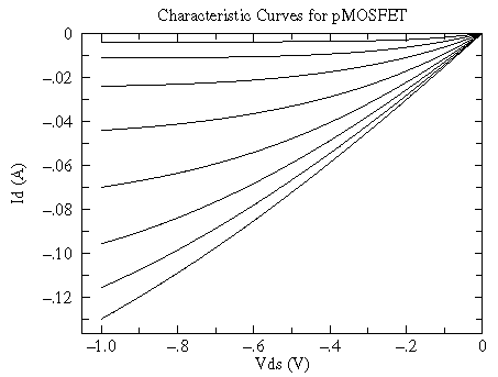
for VG = -2.0, -2.5 V, -3.0 V, ...., -5.5 V
smaller data file, postscript plot, pdf plot
Note that you can make the p-channel MOSFET characteristic curves look like the
common n-channel MOSFET curves just by rotating the pMOSFET plot by 180°. In swapping
n-channel for p-channel so nMOSFET  pMOSFET,
we've reversed the direction of current flows
(so currents are negative -- flowing out of the drain in a pMOSFET) and the
required supply voltage becomes negative for a pMOSFET.
That is to say that the p-channels are designed for negative power supplies
and out-flowing (negative) drain currents -- the opposite of n-channels.
pMOSFET,
we've reversed the direction of current flows
(so currents are negative -- flowing out of the drain in a pMOSFET) and the
required supply voltage becomes negative for a pMOSFET.
That is to say that the p-channels are designed for negative power supplies
and out-flowing (negative) drain currents -- the opposite of n-channels.
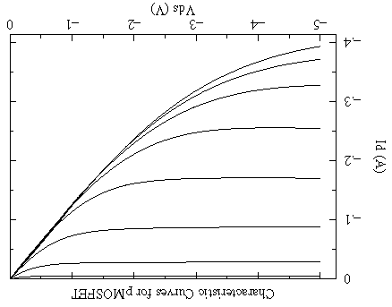
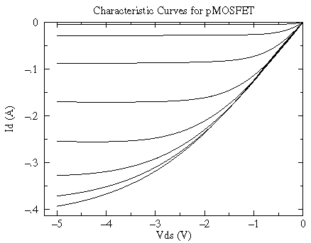
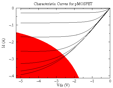
Perhaps the most striking aspect of these curves is the power being controlled by this device. At the extreme these curves display a FET with a drain current of -.4 A and a voltage drop of -5 V, which is a power dissipation of .4×5=2 Watts -- way beyond the thermal limit of the package (0.7 W). If we display the thermally disallowed region (ID×VDS > .7 W) on top of these characteristic curves you can get a better idea of how this device might be used.
The small VDS "ohmic" region and the small ID "saturation" region are available.
In the usual saturation region the characteristic curves are much like a JFETs, but now with negative controlling gate voltages:
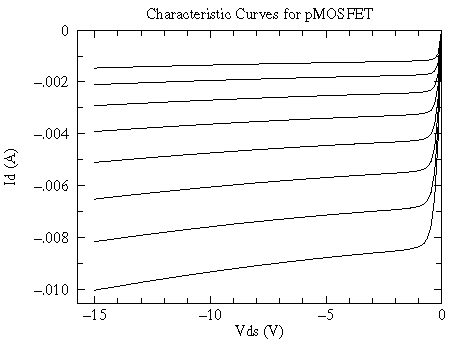
for VG = -1.80 V, 1.85 V, 1.90 V, ...., 2.15 V
big data file, smaller data file, postscript plot, pdf plot
Note the small range of VG controlling a big range of ID... these devices can be more sensitive amplifiers than JFETs.
In the small VDS "ohmic" region the characteristic curves
are nearly straight lines through the origin -- the defining behavior of
a resistor. Here the slope line is controlled by the gate voltage. As
VG0 the lines become flat: a large resistance and an "off" transistor.
For more negative VG the resistance approaches a small limiting resistance,
here about 6.7 
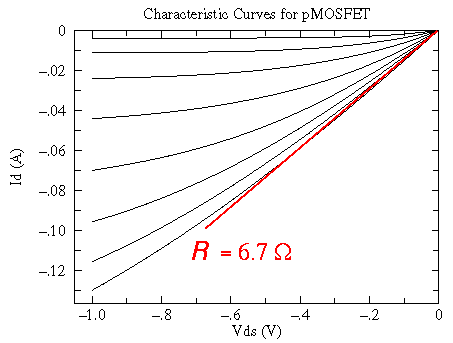
for VG = -2.00 V, -2.25 V, -2.50 V, ...., -3.75 V smaller data file, postscript plot, pdf plot
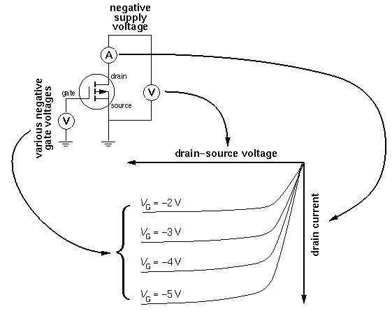
The behavior of an enhancement p-channel metal-oxide field-effect transistor (pMOSFET) is largely controlled by the voltage at the gate (usually a negative voltage). For the usual drain-source voltage drops (i.e., the saturation region: negative voltages from a few volts down to some breakdown voltage) the drain current (ID) is nearly independent of the drain-source voltage (VDS), and instead depends on the gate voltage (VG). (This is unusual behavior: usually more voltage produces to more current, but here the current only increases slightly with increasing VDS.) The transconductance, i.e., the ratio of the change in drain current to change in gate voltage, often denoted by g or yfs, is
g = yfs =
 ID/VG
ID/VG
In the simplest approximation the characteristic curves of a pMOSFET are a set of flat lines:
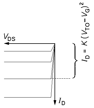
Each (flat) curve shows that ID doesn't change with changing VDS. The different levels show that ID does depend on VG. The spacing of the constant-ID curves is usually not constant, instead ID depends quadratically on VG:
ID=K(VTO-VG)2
where the threshold voltage VTO and K are constants.
A slightly more complicated approximation takes into account the sloping of the characteristic curves. In bipolar transistors this is due to the Early Voltage, here a very similar equation results from quite different physics: channel length modulation. The equation looks like:
1/VA = 
So in this model all the
characteristic curves all have a common x-axis intercept
at the large positive voltage 1/. (The dashed curves
are far from the active region and in no way represent the actual behavior of
the transistor for positive VDS. In fact, the transistor
is not designed to be operated with positive VDS.)
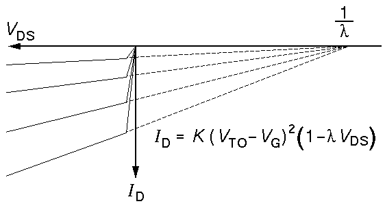
(For the above measured BS250, 1/ ranges
from 50 to 70 V.)
The actual relationship between the drain current (ID) and the controlling gate voltage (VG) and drain-source voltage drop (VDS) is some complicated function which we can denote:
ID(VG,VDS)
Like any function we can approximate it near a particular point using just the first terms of a Taylors expansion:
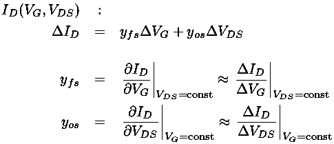
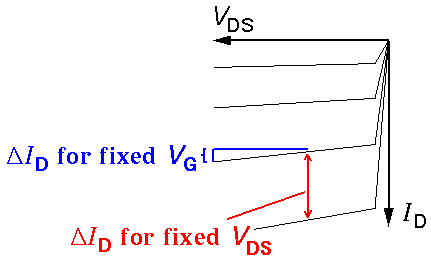
Clearly these admittance (y) parameters are not constants. For example yos is the slope of a characteristic curve, which is small for voltages near threshold and increases for larger VG.
The defining parameter -- the transconductance g or yfs -- is not at all constant. To the extent that the drain current depends quadratically on the gate voltage, the transconductance -- which is the derivative: dID/dVG -- depends linearly on VG. Below is the measured relationship: ID vs VG for the above BS250. Notice that for VG<VTO, the drain current is crudely approximated by the quadratic, whereas for VG>VTO the drain current depends approximately exponentially on VG. Thus the drain current is not strictly zero here, merely exponentially small.
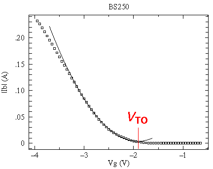
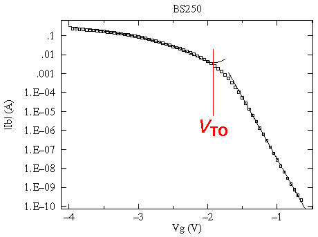
(Note that VG=0 is not in the saturation region, so the IDSS parameter is a very small current.)
The characteristic curves focus on the output of the transistor, but we can also consider the behavior of the input. In normal operation the gate is separated by an insulating layer from the rest of the transistor, and so IG is essentially zero (which should sound like a huge input resistance). As a result the outputs have little effect on the inputs, but if we follow the traditional analysis the actual functional relationship giving the gate current (IG) from the gate voltage (VG) and drain-source voltage drop (VDS) is some complicated function which we can denote:
IG(VG,VDS)
Like any function we can again approximate it near a particular point using just the first terms of Taylors expansion:
The small values of yrs and yis shows that the input is largely unaffected by the output and that the input resistance is huge. In fact this input resistance is so large that the capacitance reactance is almost always of greater significance.
Particularly for MOSFETs it should be noted that in the small VDS region -- before the saturation region -- the MOSFET characteristic curves look like nearly straight lines through the origin. VG controls the slope of these lines, so the MOSFET acts like a variable resistor with a voltage (VG) control. Here is a plot of this region for the above BS250:
The spec sheet reports the following values for the BS250:
| Characteristics | Symbol | Min | Typ | Max | Unit |
|---|---|---|---|---|---|
| Forward Transconductance | yfs | - | 150 | - | m mhos |
| Static Drain-Source On-Resistance | RDS(on) | - | - | 14 | |
| Zero-Gate Voltage Drain Current | IDSS | - | - | -500 | nA |
| Gate Threshold Voltage | VTO | -1 | - | -3.5 | V |
| Input Capacitance | CiSS | - | 60 | - | pF |